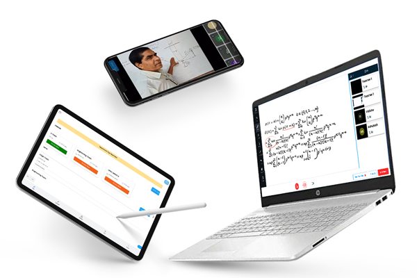
Page 1 :
PRACTICE SHEET ON SEMICONDUCTOR, DATE-10-01-22, CLASS-XII, , 1.Draw a pn junction with reverse bias? Which biasing will make the resistance of a, p-n-junction high?, , 2.Draw the voltage current characteristics of a pn junction diode?, , 3.For a extrinsic semiconductor, indicate on the energy band diagram the donor and, acceptor levels?, , 4.What do you mean by depletion region and potential barrier in junction diode?, 5.What are the advantages and disadvantages of semiconductor devices over vacuum, tubes?, , 6.The base of a transistor is lightly doped. Explain why?, , 7.What do you mean by hole in a circuit? Write its two characteristics?, , 8.In an n-type silicon, which of the following statement is true,give reason in each:, (a) Electrons are majority carriers and trivalent atoms are the dopants., , (b) Electrons are minority carriers and pentavalent atoms are the dopants., , (c) Holes are minority carriers and pentavalent atoms are the dopants., , (d) Holes are majority carriers and trivalent atoms are the dopants., , 9,Which of the statements given in question-8 is true for p-type semiconductors., 10.In an unbiased p-n junction, holes diffuse from the p-region to n-region because, (a) free electrons in the n-region attract them., , (b) they move across the junction by the potential difference., , (c) hole concentration in p-region is more as compared to n-region., , (d) All the above