Page 1 :
NANO MATERIALS, INTRODUCTION:, Nanotechnology is a multidisciplinary science and technology and, encompasses physical, chemical, biological, engineering and electronic processes. It is the study, deals with various structures of matter having dimensions of the order of billionth of a meter., These materials or particles are called as nano particle. Nano technology is the making of usage, and technique, in order to solve a problem to perform specific functions. The particles which are, smaller than about 100nm give rise to enhance properties of nano structures built from them., Matter arranged by exercising control over length of one to hundred nanometers and the, formulating structures exhibit characteristics that are specific to their size and dimensions, the, resulting materials are called nano materials., What are nanomaterials?, Nanoscale materials are defined as a set of substances where at least one dimension is, less than approximately 100 nanometers. A nanometer is one millionth of a millimeter approximately 100,000 times smaller than the diameter of a human hair. Nanomaterials, are of interest because at this scale unique optical, magnetic, electrical, and other, properties emerge. These emergent properties have the potential for great impacts in, electronics, medicine, and other fields., Classification of Nanomaterials, Nanomaterials have extremely small size which having at least one dimension 100 nm, or less. Nanomaterials can be nanoscale in one dimension (eg. surface films), two, dimensions (eg. strands or fibres), or three dimensions (eg. particles). They can exist in, single, fused, aggregated or agglomerated forms with spherical, tubular, and, irregular shapes. Common types of nanomaterials include nanotubes, dendrimers,, quantum dots and fullerenes. Nanomaterials have applications in the field of nano, technology, and displays different physical chemical characteristics from normal, chemicals (i.e., silver nano, carbon nanotube, fullerene, photocatalyst, carbon nano,, silica)., According to Siegel, Nanostructured materials are classified as Zero dimensional, one, dimensional, two dimensional, three dimensional nanostructures., Nanoparticles are particles between 1 and 100 nanometers in size. In nanotechonology a, particle is defined as a small object that behaves as a whole unit with respect to its, transport and properties. Particles are further classified according to diameter. Ultrafine, particles are the same as nanoparticles and between 1 and 100 nanometers in size. Coarse, particles cover a range between 2,500 and 10,000 nanometer. Fine particles are sized, between 100 and 2,500 nanometers. Nanoparticles research is currently an area of intense, scientific interest due to a wide variety of potential applications in biomedical, optical and, electronic fields
Page 2 :
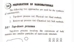
SIZE DEPENDENT PROPERTIES, a) Surface area: Nanomaterials have a significant proportion of atoms existing at the surface., Properties like catalytic activity, gas adsorption and chemical reactivity depend on the surface, area. Therefore nanomaterials can show specific related properties that are not observed in bulk, materials., b) Electrical properties: the electronic bands in bulk materials are continuous due to, overlapping of orbitals of billion of atoms. But in the nanomaterials, very few atoms or, molecules are present so the electric band becomes separate and the separation between different, electric stated varies with the size of the nanomaterials. Hence, some metals which are good, conductors in bulk semiconductors and insulator as their size is decreased to nano level., c) Optical properties: Nanomaterials have particular optical properties as a result of the way, , light intersects with their fine nanostructures. The discrete electronic states of nanomaterials, allow absorption and emission of light at specific wavelength. Hence, nanomaterials exhibit, unique color different from bulk materials., , d)Thermal Properties: Decrease in size increases the surface energy, decreases the melting pt,, this is because surface atoms require less energy to move because they are in contact with less, number of atoms of the substance., Ex: Silicon nanowire possesses less thermal conductivity than bulk silicon., SYNTHESIS OF NANOMATERIALS, There are two methods of preparing nanomaterials. One is top-down approach & the other is, bottom-up approach., , , In top-down approach, the material is reduced from bulk size to nano scale., Examples, for top-down approach are ball milling method & nanolithography., , , In bottom-up approach, matter in atomic or molecular level gets assembled to form tiny, clusters, which grow to reach nano-size., , Examples for bottom-up approach are arc discharge method, chemical vapor deposition, physical, vapor deposition & sol gel method.
Page 3 :
Nanomaterial synthesis by SOL – GEL PROCESS:, Sol gel processes principle is conversion of precursor solution into gel via hydrolysis and, condensation reactions., The following steps are involved in the synthesis of nanomaterials by sol-gel process., , Nanoparticles, Examples: Zinc oxide nanoparticles, TiO 2 nanoparticles can be synthesized by this method., a) preparation of sol: In this method, metal alkoxide is used a precursor to, synthesis nanoparticles of a metal oxide. Metal alkoxide is dissolved in alcohol and, then water is added under acidic, neutral or basic conditions. Addition of water leads, to hydrolysis in which alkoxide ligand is replaced with a hydroxyl ligand., MOR + H 2 O→ MOH + ROH (hydrolysis), b) Conversion of sol to gel : The polycondensation reaction between MOH and MOR, results in the formation of an oxide – or alcohol – bridged network(gel)., MOH+ ROM → M- O –M +R-OH (Polycondensation), c) Aging of the gel: The reaction mixture is allowed to continue polycondensation, reactions until the gel transforms into a solid mass, accompanied by contraction, of the gel network and expulsion of solvent from gel pores., d) Removal of a solvent: The water and other volatile liquids are removal from the, gel network. If isolated by thermal evaporation, the resulting product is termed a, xerogel. If the solvent is extracted under supercritical conditions, resulting product is, termed an aerogel., e) Heat treatment: The sample obtained is calcined at high temperature (8000C), to obtain nanoparticles.Nanoparticles formed by sol-gel process commonly have a, size ranging from 1 to 100 nm., , 1., 2., 3., 4., , Advantages, Nanomaterials of high purity with good homogeneity can be obtained., Samples can be prepared at lower temperature., Easy to control synthesis parameters to control physical characteristics like shape and, size of resulting materials., Simple and inexpensive equipment.
Page 4 :
PRECIPITATION METHOD, Principle: The principle involved in the precipitation of precursor materials at constant pH via, condensation. Precipitation method can be used to prepare nanoparticles of metal oxides, metal, sulphides and metals., Process, a) In this method, an inorganic metal salt (such as nitrate, chloride or acetate of, metal) is dissolved in water (precursor solution)., b) Metal cations exist in the form of metal hydrate species, for example,2 (Al, (H O), 6, 3+, 3+, ) or (Fe(H 2 O) 6 ) ., c) These metal hydrates are added to precipitating agent like NaOH or NH4OH, it, changes the pH & causes condensation of precursor., d) Thus concentration of solution increases and reaches a critical level called super, saturation. At this concentration nucleus formation is initiated. The nucleus further, grows into, particles,, which gets, precipitate., The, precipitate, obtained, is filtrated,, washed, with water, air dried and finally calcined at high, temperature, , Advantages: The process is relatively economical., The wide range of single and multi components to oxide nano powders can be synthesized., CHEMICAL VAPOUR DEPOSITION (CVD):, CVD is a process where gaseous precursors react to form a solid coating on a heated substrate.
Page 5 :
NANO SCALE MATERIAL, Nano scale materials are defined as a set of substances where atleast one dimension is less than, approximately 100nm. A nanometer is one millionth of a millimeter. Nano materials are of, interest because of this scale unique optical, magnetic, electrical and other properties emerge., These emergent properties have the potential for great impacts in electronics, medicine and other, fields., FULLERENES: Fullerenes are class of molecules made of only, carbon atoms having closed cage like structure. Many number of, fullerene molecules with different carbon atoms like C60, C70, C74,, C76 etc.., have been prepared but C60 is more stable. The C60, molecule had spherical shape resembling a soccer ball (foot ball). The, most important fullerene is C60 containing 60 carbon atoms, which are commonly known as Buckminster fullerene. The name, of Buckminster fullerene comes from the name of an architect, Richard Buckminster fuller who had built the geodesic dome with, spherical shape. The C60 molecule consist of 12 pentagons and 20, hexagons. and each pentagon is surrounded by five hexagons and each, hexagon is surrounded by three hexagons . The chemical formula for, fullerene is C20+2n., , Properties of fullerenes, 1. Fullerenes are heat-resistant and unique, insoluble in water, dissolve in organic solvents., 2. In fullerenes, 12 pentagonal rings are necessary and sufficient to affect the cage closure., 3. Fullerenes C60 molecule can absorb more than 100 photons in a nano second and transfer, that energy (230V) to its vibrational energy., 4. Highest tensile strength of any known 2D structure or element., 5. Highest packing density of all known structures., 6. Impenetrable to all elements under normal circumstances, even to, a helium atom with energy of 5 eV., Applications:, 1. Fullerenes are extremely flexible and strong nature, therefore are being considered, for use in combat armor. It is used in electrographic imaging, solar cells, non linear, optical thin films., 2. Researchers have found that water-soluble derivates of fullerenes inhibit the HIV-1, protease (enzyme responsible for the development of the virus) and are therefore useful in, fighting the HIV virus that leads to AIDS., 3. Elements can be bonded with C 60 or other fullerenes to create more diverse material, including superconductors and insulators., 4. Used for the conversion of diamondUsed as gas sensors, temperature sensors, particle sensors, and detection of organic vapors., CARBON NANO TUBES:, Carbon nanotubes are allotropes of carbon with a cylindrical nanostructure having diameter of, 1nm and longer than a micrometer. It is one dimensional material like nano wires. CNT is made, up of graphite sheet. When the graphite sheet is rolled up hexagonally, it forms a tube like, structure is called as CNT. Types of CNT:, 1. Single-Walled CNT(SWCNTs): They are formed by rolling up of single, graphine layer. The diameter of SWCNT is 1-4nm and length can go up to few, micrometers.
Page 6 :
2. Multi-Walled CNT(MWCNTs):They consist of two or more concentric graphine, cylindres with vander wall’s forces between adjacent tubes. The diameter of, MWCNTs is in the range of 30-50nm and length can go up to few micrometers., , Properties and applications:, 1. CNTs exhibit high electrical and thermal conductivty. They have low density and very high, mechanical strength due to these properties they are used as electrode material for lithium ion, rechargeable batteries., 2. CNTs can emit electrons when subjected to high electrical field due to this property they are, used in the field emission X-ray tubes., 3. The CNTs are about 20 times stronger than steel and hence find applications in making, automobiles and aircraft body parts., 4. SWCNTs absorb radiation in the near IR range (700-1100nm) and convert it to heat. This, property is used in caner thermotherapy to selectivity kill cancer cells without affecting nearby, healthy tissues., GRAPHENES, Graphne is a semi-metal with small overlap between the valence and conduction bands. It is, an allotrope of carbon consisting of single layer of carbon atoms arranged in a hexagonal, lattice. Graphene has a sp2 hybridized planar honey comb lattice structure with zero energy, band gap. It is a pure carbon in the form of a very thin, nearly transparent sheet, one atom, thick. Graphene can be described as a one-atom thick layer of graphite., Properties:, Graphenes have high electrical conductivity, large surface area, high mechanical and thermal, stability., One of the useful properties of graphene is that it is zero-overlap semi-metal (with both holes and, electrons as charge carriers) with very high electrical conductivity., Applications, Pencil production, coatings, lubricants, paint production, batteries, high performance adsorbent, for water pollution, efficient photocatalyst, high performance fuel cell catalyst.


